7404 IC: Comprehensive Guide on Datasheet, Pin Diagram, Applications

What is the 7404 IC?
The 7404 IC, commonly known as SN7404 hex inverter, it is a hex inverter integrated circuit commonly used in digital electronics. As a member of the 7400 series of integrated circuits, it plays a critical role in various logic gate designs.
The 7404 IC is a hex inverter, meaning it contains six individual inverter gates. In digital logic, an inverter, or NOT gate, is a fundamental building block that outputs the opposite logic level to its input. For instance, if the input is a logic high (1), the output will be a logic low (0), and vice versa. The 7404 IC is part of the TTL (Transistor-Transistor Logic) family, known for its high speed and reliability. Understanding the 7404 IC is crucial for anyone involved in digital logic design due to its widespread application and fundamental role in digital circuits.

Why is the 7404 IC Important to Digital Circuits?
The 7404 IC is vital in digital circuits as it inverts input signals, a basic but essential function in various logic operations. In logic gate designs, the 7404 IC can be employed to construct more complex gates like NAND, NOR, XOR, and XNOR gates. By combining inverters with other basic gates, designers can create intricate logic functions required for digital processing. The hex inverter configuration of the 7404 IC allows for multiple inverting operations within a single package, optimizing space and power consumption in circuits.
The SN7404 integrated circuit has a total of 14 pins, divided into two rows, each row of 7 pins. Each pin has a specific function, with inputs and outputs arranged in pairs corresponding to each of the six inverters. Below is the pin configuration:
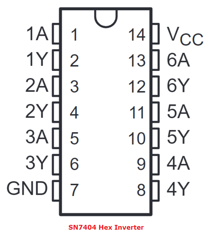
In it, the pins of the left row are GND (ground), 1A, 1Y, 2A, 2Y, 3A, 3Y, and the pins of the right row are VCC (power supply), 4A, 4Y, 5A, 5Y, 6A, 6Y. A indicates the input port and Y indicates the output port. VCC and GND are used to supply power to the chip respectively. Here is a detailed description of each pin.
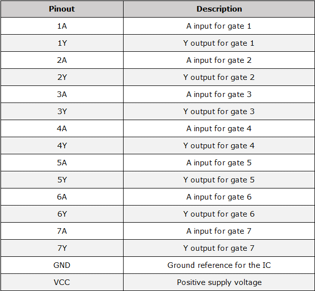
(Pin description)
These pins are welded to the circuit board, allowing the integrated circuit chip to function properly. Properly connecting these pins ensures the 7404 IC functions correctly within a circuit. Its packaging form has DIP (double in-line) and SOIC (small outer packaging), users can choose the appropriate packaging according to actual needs. Download its datasheet here: SN7404 Datasheet
What Are the Specifications of 7404 Hex Inverter?
Supply voltage: 4.75V to 5.25V
Input voltage: 0V to 5V
Output voltage: 0V to 5V
Maximum power Dissipation: 500mW
Propagation delay: Approximately 10ns
Operating temperature range: 0°C to 70°C
Storage temperature range: -65°C to 150°C
Noise margin: 0.4V for both HIGH and LOW logic levels
Key Features of the 7404 Hex Inverter
Six Independent Inverters
The 7404 IC includes six separate inverters, allowing for multiple logic inversion operations within a single package. This enables to improve the circuit design efficiency and reduces component count.
TTL Compatibility
As a TTL logic gate, the 7404 Hex Inverter is compatible with other TTL devices. You can seamlessly integrate it into existing TTL-based systems. This compatibility is crucial for maintaining consistent logic levels and signal integrity.
High Switching Speed
You can see the specifications of the 7404 Hex Inverter as above, it has a very high switching speed, typically operating in the nanosecond range. It means it is well-suited for any high-frequency applications where quick signal processing is essential.
Wide Operating Voltage Range
The 7404 Hex Inverter has widely applications in power supply environments. Because it can operate within a voltage range of 4.75V to 5.25V, with 5V being the typical operating voltage.
Low Power Consumption
Despite its high switching speed, the 7404 IC consumes relatively low power, so it is a go-to choice for battery-powered and energy-sensitive applications.
How the 7404 IC Operates?
The 7404 IC operates by utilizing transistor-transistor logic technology to achieve inversion. When a high voltage is applied to the input, the corresponding transistor switches on, pulling the output to ground (logic low). Conversely, a low input voltage keeps the transistor off, allowing the output to be pulled up to the supply voltage (logic high).
Applications of 7404 Hex Inverter
In our daily life, the 7404 IC can be found in devices like computers, communication systems, and control systems. For example, it may be used to invert control signals in a microprocessor system or to generate clock pulses for timing purposes. Some other common applications including:
Microcontroller Systems
In microcontroller-based systems, the 7404 IC can invert control signals, generate clock pulses, and convert logic levels to ensure proper operation and communication between components.
Communication Systems
The IC is used in communication systems to create complementary signals for differential transmission, improve signal integrity, and filter out noise.
Timing Circuits
The 7404 IC is employed in timing circuits to generate precise clock signals and oscillations required for synchronous operations in digital systems.
Computational Devices
In computational devices, the IC is used for data inversion, error detection, and parity generation, enhancing the reliability and accuracy of digital computations.
Basic Circuit Implementation of 7404 IC
A basic circuit using the 7404 IC involves connecting the power supply to the Vcc and GND pins and using any of the input-output pairs for the NOT gate functionality. For example, connecting an input signal to Pin 1 and taking the output from Pin 2 provides an inverted signal.
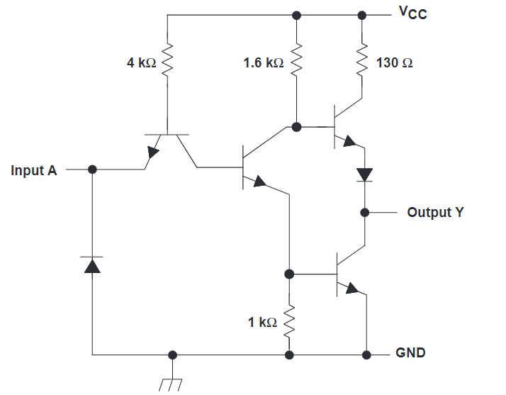
(7404 IC circuit diagrams)
Complex Circuit Designs Using 7404 IC
More complex designs might use multiple inverters within the 7404 IC to create multi-stage logic circuits, such as oscillators, frequency dividers, or combinational logic circuits. These designs leverage the 7404 IC's ability to invert and buffer signals efficiently.
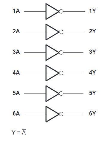
(Positive logic diagram of 7404 IC)
Truth Table of the 7404 IC
A truth table is a tabular representation of the input-output relationship of a digital logic gate. For the 7404 IC, each inverter's operation can be summarized in a simple truth table as shown below.

Explanation of the Truth Table
Input (A): This column represents the logic level applied to the input pin of each inverter within the 7404 IC.
Output (Y): This column represents the resulting logic level at the output pin of the corresponding inverter.
The 7404 IC inverts the logic level of its input signal:
When the input (A) is 0 (LOW), the output (Y) is 1 (HIGH).
When the input (A) is 1 (HIGH), the output (Y) is 0 (LOW).
7404 IC vs 7408 IC
The 7404 IC is a hex inverter, whereas the 7408 IC is a quad two-input AND gate. While both ICs are used in digital logic design, their functions are different. The 7404 IC inverts input signals, while the 7408 IC performs logical AND operations on pairs of inputs.
How to Test the 7404 IC?
Testing the 7404 IC involves verifying its functionality using a simple circuit. By applying known input signals and measuring the outputs, you can determine if the IC is working correctly. Tools like multimeters and oscilloscopes are commonly used for this purpose. Here is a step-by-step testing guide.
Equipment Needed
7404 IC
PCB (printed circuit board)
Power supply (5V)
Digital multimeter
Signal generator (optional)
Connecting wires
LEDs and resistors (optional for visual testing)
Steps to Test the 7404 IC
Step 1: Visual Inspection
a. Check for physical damage, inspect the 7404 IC for any visible signs of damage, such as cracks or burnt marks.
b. Verify pin connections, make sure all pins are straight and not bent or broken.
Step 2: Set Up the Test Circuit
a. Insert the 7404 IC into the PCB boar, place the IC in the PCB and ensure each pin is properly seated.
b. Connect the Vcc pin (Pin 14) to the +5V supply and the GND pin (Pin 7) to the ground of the power supply.
Step 3: Testing Each Inverter
a. Choose one of the six inverters in the 7404 IC (e.g., 1A and 1Y for the first inverter).
b. Connect a signal to the input pin of the selected inverter (e.g., 1A). You can use a signal generator to apply a HIGH (5V) or LOW (0V) logic level. Alternatively, you can use a simple toggle switch or directly connect to Vcc or GND.
c. Use a digital multimeter to measure the voltage at the corresponding output pin (e.g., 1Y). Alternatively, you can connect an LED with a current-limiting resistor to visually observe the output.
Step 4: Verify Logic Levels
a. Input LOW (0V):
Apply 0V to the input pin (e.g., 1A).
Check the output pin (e.g., 1Y) with the multimeter or LED. The output should be HIGH (close to 5V).
b. Input HIGH (5V):
Apply 5V to the input pin (e.g., 1A).
Check the output pin (e.g., 1Y) with the multimeter or LED. The output should be LOW (close to 0V).
Step 5: Repeat for All Inverters
Repeat Steps 3 and 4 for the other five inverters in the IC (2A/2Y, 3A/3Y, 4A/4Y, 5A/5Y, 6A/6Y) to ensure all inverters are functioning correctly.
Step 6: Optional Signal Generator Test
Use a signal generator to apply a continuous square wave signal to the input pin. And observe the output pin using an oscilloscope to verify the inversion of the signal.
Troubleshooting Tips
l No Output: If there is no output, check the power supply connections and ensure the IC is correctly seated in the breadboard.
l Incorrect Logic Levels: Verify the input signal levels and ensure they are within the specified voltage range for TTL logic (0V for LOW, 5V for HIGH).
l Intermittent Operation: Ensure stable connections and check for any loose wires or poor contacts on the breadboard.
Frequently Asked Questions (FAQs)
Q1: What is the 7404 IC used for?
A: The 7404 IC is primarily used for signal inversion in digital circuits. It takes an input signal and outputs its logical inverse. This functionality is essential in various applications, such as creating timing signals, buffering, and implementing specific logic functions.
Q2: How do I connect the 7404 IC in a circuit?
A: To connect the 7404 IC in a circuit, follow these steps:
1. Connect the Vcc pin (Pin 14) to the positive power supply (typically +5V).
2. Connect the GND pin (Pin 7) to the ground.
3. Connect the input signals to the designated input pins (Pins 1, 3, 5, 9, 11, 13).
4. Obtain the inverted output signals from the corresponding output pins (Pins 2, 4, 6, 8, 10, 12).
Q3: What are the alternatives to the 7404 IC?
A: Alternatives to the 7404 IC include other inverter ICs like the CD4069, which operates at a wider voltage range, and the 74LS04, a low-power variant of the 7404 IC. Additionally, CMOS-based inverters such as the 74HC04 offer higher speed and lower power consumption.
Here is the all we shared today about the 7404 IC, and hope this is useful for you to better understand and choose a suitable one for your projects. If you are looking for a reliable component supplier, whatever for the 7404 hex inverter or other integrated circuits, IGBT chips or connectors, consider partnering with Jinftry. We are a trusted supplier known for superior quality and exceptional customer service. And we believe we can provide what you want.
Statement
All articles (images, texts, audio) on this site are uploaded and shared by users, or integrated from relevant internet sources, only for user's learning. If your rights are violated, please contact the administrator to delete! Link to this article: https://www.jinftry.com

