IC 7404 Pin Diagram, Equivalents and Applications

The 7404 IC is a hex inverter, which is renowned for its versatility, ranging from simple logic circuit extensions to complex pulse generators and power inverters. Its high reliability and low energy consumption make it a preferred choice for battery-powered devices.
This inverter features a straightforward, user-friendly design, adheres to a standard pin layout, and seamlessly integrates with a single 5V power supply, facilitating its use in various circuits from breadboard prototypes to DIY electronics projects. In this article, we will provide detailed information about the 7404 integrated circuits, including pin configuration, circuit characteristics, truth tables, and equivalent models.
7404 Integrated Circuit Introduction
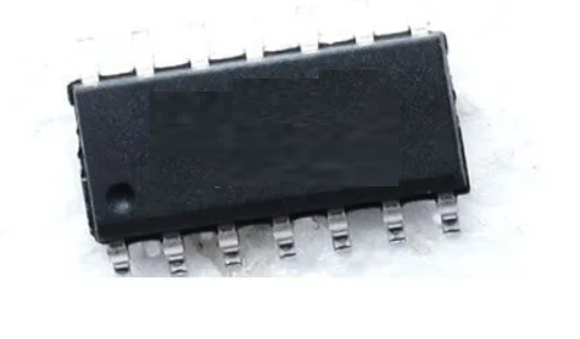
The 7404 Hex Inverter, part of the 7400 series, is specifically used as a hex inverter. It is widely used in various electronic circuits due to its simplicity and reliability. The primary function of the 7404 IC is to invert the input signal; if the input is high, the output will be low, and vice versa. This characteristic makes it indispensable in digital logic design.
This device contains six independent inverters, each with an input and an output, optimized to operate within a 5-volt power range and handle currents up to 40 milliamps. Its multifunctionality is further emphasized through the availability of multiple packaging options, including the widely used DIP and the compact SOIC packaging.
Features and Specifications of IC 7404
Six Inverted Outputs: The 7404 IC has six inverters in one package, making it highly effective for complex circuits that require multiple inversions simultaneously.
Compatible Output Connections: The IC's outputs are compatible with CMOS, NMOS, and TTL logic families, enabling easy integration into various digital systems, thereby reducing complexity and enhancing reliability.
Wide Operating Voltage Range: Typically operates between 4.75V to 5.25V, it is a well-suited component for various digital systems.
Temperature Range: Operates reliably within a temperature range of -70°C to +70°C, can withstand various temperature changes.
Parameter Specifications of 7407 Hex Inverter
Maximum current output: 8mA
Power supply voltage range: +4.75V to +5.25V
Operating temperature range: -70°C to +70°C
Storage Temperature: -65°C to 150°C
Maximum supply voltage: +7V
Input Voltage: 0V to 5.5V (maximum)
Output Voltage: 0V to 5V
Input Current: 1µA to 1.6mA
Output Current: 16mA (source or sink)
Propagation Delay: Approximately 12ns
Maximum rise time: 15ns
Maximum fall time: 15ns
Output type: TTL
Logic type: Bipolar
Package Type: Available in 14-pin DIP, SOIC.
IC 7404 Pin Diagram
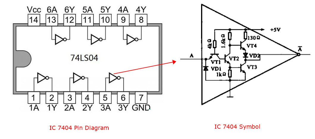
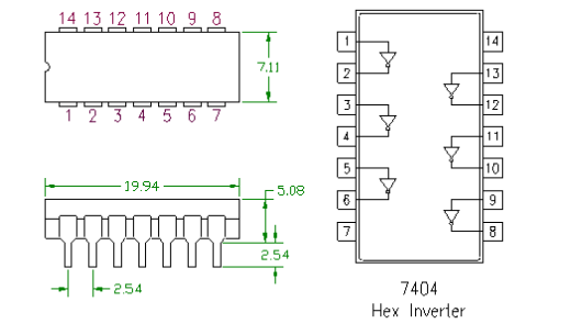
Pin 1: A input for gate 1
Pin 2: Y output for gate 1
Pin 3: A input for gate 2
Pin 4: Y output for gate 2
Pin 5: A input for gate 3
Pin 6: Y output for gate 3
Pin 7: Ground
Pin 8: Y output for gate 4
Pin 9: A input for gate 4
Pin 10: Y output for gate 5
Pin 11: A input for gate 5
Pin 12: Y output for gate 6
Pin 13: A input for gate 6
Pin 14: Positive power supply
How Does IC 7404 Hex Inverter Work?
Each NOT gate operates by inverting the input logic level, providing an output that is the logical complement of the input. Its fundamental operation is simple: if the input is high (logic level 1), the output will be low (logic level 0), and if the input is low (logic level 0), the output will be high (logic level 1). This operation is governed by the basic truth table for a NOT gate:
|
Input (A) |
Output (Y) |
|
0 |
1 |
|
1 |
0 |
This truth table highlights the inverting nature of the NOT gate. Specifically, when the input (A) is 0, the output (Y) is set to 1, and vice versa, when the input is 1, the output switches to 0. This binary opposition between input and output underscores the inverter's role in digital circuits, where flipping signal states is necessary for logic operations.
Internal Structure of 7404 IC
The internal structure of each NOT gate within the IC 7404 consists of a series of transistors configured to perform the inverting function. Here's a simplified explanation of the internal workings:
1. Transistor Configuration
Each inverter in the 7404 uses a pair of transistors, typically NPN and PNP types, arranged in a common emitter configuration. When the input signal is applied to the base of the NPN transistor, it controls the conduction state of the transistor.
2. Inversion Process:
When the input is high (logic 1), the NPN transistor turns on, causing current to flow from the collector to the emitter. This current flow pulls the output voltage down to ground (logic 0).
When the input is low (logic 0), the NPN transistor is off, and the PNP transistor in the pull-up configuration ensures that the output is pulled up to the supply voltage (logic 1).
3. Voltage Levels
The IC 7404 operates with standard TTL voltage levels. Typically, a voltage around 0V to 0.8V represents a logic 0, and a voltage around 2V to 5V represents a logic 1. These voltage thresholds ensure reliable switching and compatibility with other TTL logic devices.
Equivalents to IC 7404
There are many versions of the 74×04 chip. They all have the same functionality but with different specifications such as supported voltages and maximum current output. To make it easy to identify, some manufacturers also add a prefix, such as the SN74HC04 and SN74LS04 by Texas Instruments. Here are some alternatives and equivalents of IC 7404 hex inverter:
74HC04
Description: A high-speed CMOS version of the 7404, designed for faster operation and lower power consumption.
Operating Voltage: 2V to 6V
Propagation Delay: Approximately 10ns
Output Current: Up to 25mA
Package Types: DIP, SOIC, TSSOP
74HCT04
Description: A high-speed CMOS version that is TTL compatible, ensuring interoperability with TTL logic levels.
Operating Voltage: 4.5V to 5.5V
Propagation Delay: Approximately 13ns
Output Current: Up to 25mA
Package Types: DIP, SOIC, TSSOP
74LS04
Description: A standard TTL version with high-speed operation and low power consumption.
Operating Voltage: 4.75V to 5.25V
Propagation Delay: Approximately 12ns
Output Current: Up to 16mA
Package Types: DIP, SOIC
74LVC04
Description: A low voltage TTL version suitable for modern low power applications.
Operating Voltage: 1.65V to 3.6V
Propagation Delay: Approximately 6ns
Output Current: Up to 24mA
Package Types: DIP, SOIC, TSSOP
74AC04
Description: An advanced CMOS version offering higher speed and lower power consumption.
Operating Voltage: 2V to 6V
Propagation Delay: Approximately 5ns
Output Current: Up to 24mA
Package Types: DIP, SOIC, TSSOP
74ALS04
Description: An advanced low-power Schottky TTL version, offering improved speed and power efficiency.
Operating Voltage: 4.5V to 5.5V
Propagation Delay: Approximately 8ns
Output Current: Up to 8mA
Package Types: DIP, SOIC
74F04
Description: A very high-speed TTL version designed for applications requiring extremely fast operation.
Operating Voltage: 4.5V to 5.5V
Propagation Delay: Approximately 4ns
Output Current: Up to 20mA
Package Types: DIP, SOIC, TSSOP
74C04
Description: A CMOS version similar to the 4000-series, offering flexibility and low power consumption.
Operating Voltage: 3V to 15V
Propagation Delay: Approximately 100ns
Output Current: Up to 10mA
Package Types: DIP, SOIC
Applications of 7404 Hex Inverter
The 7404 Hex Inverter is a very key component that is widely used in every almost electronic circuits and systems. Its efficient logic inversion capability makes it suitable for a variety of applications.
Signal Inversion
One of the primary uses of the 7404 IC is to invert digital signals. This is crucial in digital circuits where the logic state needs to be reversed, such as inverting the output of a microcontroller to match the input requirements of other devices.
Oscillator Circuits
The 7404 Hex Inverter can be used to create oscillator circuits by configuring one of its inverters with feedback components. This configuration can generate square waves, which are used as clock signals for timing purposes in digital circuits.
Waveform Generation
By using the 7404 hex inverter in combination with other components, it can generate various waveform patterns. For instance, it can produce square waves and pulse-width modulation (PWM) signals, which are useful in applications like motor control and signal processing.
Logic Gate Implementation
The 7404 IC can be combined with other logic gates to create more complex logic functions. For example, using NOT gates alongside AND, OR, or NAND gates allows the implementation of various logical operations necessary in digital design.
Noise Filtering
IC 7404 NOT gate can help filter out noise in digital signals. By inverting and conditioning noisy inputs, it can produce clean outputs, which is especially useful in debounce circuits for buttons and switches to prevent multiple detections from a single press.
LED Drivers
The 7404 is often used to drive LEDs by inverting control signals. This allows for straightforward LED indication of various states in a circuit, providing visual feedback for the operation of different components.
Control Systems
The 7404 is used in control systems to invert signals that manage different functions. For example, it can control relays by inverting the control signals, thereby enabling or disabling specific operations in a circuit.
IC 7404 Dimension Drawing
IC 7404 Datasheet
Want know more about IC 7404? Click here to download its datasheet: 74LS04 Datasheet
FAQs
What is the significance of the 'Hex' in 'Hex Inverter'?
'Hex' indicates that the IC contains six (hex) independent NOT gates. Each gate operates separately, allowing the IC to invert six different signals simultaneously.
How should the IC 7404 be oriented when placing it on a PCB?
The IC 7404 should be oriented such that pin 1 is correctly aligned with the pin 1 mark on the PCB. Pin 1 is usually marked by a dot or a notch on the IC package. Ensuring correct orientation is crucial for proper operation.
What is the typical power consumption of the IC 7404?
The IC 7404 has low power consumption, typical of TTL devices. The exact power consumption depends on the operating conditions and the number of active gates, but it is generally designed to be efficient.
What is the difference between IC 7404 and IC 7408?
IC 7404 and IC 7408 are both digital logic ICs, but one is Hex Inverter and another is Quad 2-input AND gate, and they serve different functions.
Related Content:
1. IC 741 Op Amp: Pin Diagram, Working & Equivalents
2. IC 7408 Logic Gate Chip: Pin Diagram and Truth Table
3. CR2450 Button Cell Battery: Introduction, Equivalency, and CR2450 vs. CR2032
Statement
All articles (images, texts, audio) on this site are uploaded and shared by users, or integrated from relevant internet sources, only for user's learning. If your rights are violated, please contact the administrator to delete! Link to this article: https://www.jinftry.com

