IC 7408 Logic Gate Chip: Pin Diagram and Truth Table

What is 7408 Integrated Circuit?
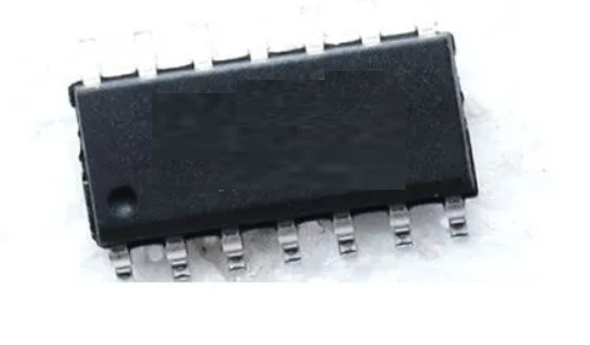
The 7408 Integrated Circuit (IC) is a quad two-input AND gate device. This means it houses four separate AND gates within a single chip. It belongs to the 7400 series of digital logic ICs, which are known for their robustness and widespread use in various electronic applications. The 7408 IC is built using Transistor-Transistor Logic (TTL) technology, ensuring fast operation and reliable performance in digital circuits.
Each AND gate within the 7408 IC takes two binary inputs and produces a single binary output. The output is high (logic level 1) only when both inputs are high. This basic logical function is foundational in digital electronics, where AND gates are used to perform operations such as enabling signals, creating specific logical conditions, and more.
What is 74 in 7408 IC?
The "74" in 7408 indicates that the IC is part of the 7400 series, a popular family of TTL logic ICs developed by Texas Instruments in the 1960s. The 7400 series is renowned for its versatility, speed, and ease of use, making it a standard in digital electronics.
The number "08" specifically identifies the IC as a quad two-input AND gate. The numbering system helps in quickly identifying the function and family of the IC. The 7400 series includes various other logic functions, such as NAND gates (7400), OR gates (7432), and flip-flops (7474), each with a unique number indicating its specific logic function.
IC 7408 Pin Diagram
The IC 7408 is a quad two-input AND gate integrated circuit with a standard 14-pin Dual In-line Package (DIP). Each pin on the IC has a specific function, as described below:
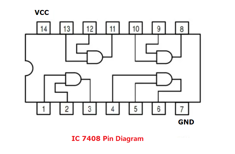
Pin functions:
|
No. |
Function |
|
Pin 1 |
Input 1 of Gate 1 |
|
Pin 2 |
Input 2 of Gate 1 |
|
Pin 3 |
Output of Gate 1 |
|
Pin 4 |
Input 1 of Gate 2 |
|
Pin 5 |
Input 2 of Gate 2 |
|
Pin 6 |
Output of Gate 2 |
|
Pin 7 |
Ground (GND) |
|
Pin 8 |
Input 1 of Gate 3 |
|
Pin 9 |
Input 2 of Gate 3 |
|
Pin 10 |
Output of Gate 3 |
|
Pin 11 |
Input 1 of Gate 4 |
|
Pin 12 |
Input 2 of Gate 4 |
|
Pin 13 |
Output of Gate 4 |
|
Pin 14 |
Positive Supply Voltage (Vcc) |
7408 IC AND Gate Truth Table
The 7408 IC contains four independent two-input AND gates. The function of each AND gate can be described using a truth table, which outlines the possible input combinations and their corresponding outputs.
Here’s the truth table for a single two-input AND gate within the 7408 IC:
|
Input 1 |
Input 2 |
Output |
|
0 |
0 |
0 |
|
0 |
1 |
0 |
|
1 |
0 |
0 |
|
1 |
1 |
1 |
In this truth table:
l 0 (Low): Represents a logic level 0, typically 0V.
l 1 (High): Represents a logic level 1, typically 5V.
1. When both Input A and Input B are low (0), the output is low (0).
2. When Input A is low (0) and Input B is high (1), the output is low (0).
3. When Input A is high (1) and Input B is low (0), the output is low (0).
4. When both Input A and Input B are high (1), the output is high (1).
This logical behavior is consistent across all four AND gates within the 7408 IC. Each gate will produce a high output only when both of its inputs are high.
If you need to use one of the AND gates in the 7408 IC for a specific logic function, here's an example:
1. Gate 1:
Inputs: Pin 1 (Input A) and Pin 2 (Input B)
Output: Pin 3
To use this gate:
Connect your first input signal to Pin 1.
Connect your second input signal to Pin 2.
The result of the AND operation will be available at Pin 3.
You can follow a similar approach for the other three gates in the IC.
The 7408 IC AND gate truth table is fundamental in understanding how this IC operates. By ensuring that both inputs are high, you can achieve a high output.
What is the Operating Voltage of 7408?
The operating voltage of the 7408 IC typically ranges from 4.75V to 5.25V, with a nominal value of 5V. This voltage range is standard for TTL logic devices, which the 7400 series, including the 7408, belongs to.
Operating within this voltage range ensures that the IC performs correctly and reliably. Exceeding the maximum voltage can damage the IC, while operating below the minimum voltage can result in unreliable or incorrect logic levels.
Features of 7408 IC
Number of Gates: 4 independent two-input AND gates
Supply Voltage: 4.75V to 5.25V
Operating Temperature: 0°C to 70°C
High Speed
Noise Immunity
Low Power Consumption: Belongs to the TTL logic family
Fan-Out Capability: Can drive multiple inputs of other TTL ICs
Input Protection: Safeguarded against static discharge and voltage spikes
Standard 14-Pin DIP Package
Wide Availability and Cost-Effectiveness
How to Connect IC 7408?
Connecting the IC 7408 in a circuit involves understanding its pin configuration and ensuring proper power supply and grounding. Here’s a step-by-step guide to connecting the IC 7408:
1. Power Supply: Connect Pin 14 to the positive supply voltage (typically 5V for TTL ICs).
2. Grounding: Connect Pin 7 to the ground (0V).
3. Inputs and Outputs: The remaining pins are used for the inputs and outputs of the AND gates:
l Gate 1: Inputs at Pin 1 and Pin 2, Output at Pin 3.
l Gate 2: Inputs at Pin 4 and Pin 5, Output at Pin 6.
l Gate 3: Inputs at Pin 9 and Pin 10, Output at Pin 8.
l Gate 4: Inputs at Pin 12 and Pin 13, Output at Pin 11.
To connect an AND gate, wire the inputs to the respective input pins (e.g., Pin 1 and Pin 2 for Gate 1) and take the output from the corresponding output pin (e.g., Pin 3 for Gate 1). Ensure that the inputs are at the correct logic levels (high or low) for the desired operation.
What is the IC 7408 Equivalent To?
The IC 7408 can be considered equivalent to other quad two-input AND gate ICs in terms of functionality, though there may be differences in the underlying technology or specifications. Some equivalent ICs include:
1. CD4081
This is a CMOS version of the quad two-input AND gate, which operates at a wider voltage range (3V to 15V) compared to the 7408. It is suitable for low-power applications and is often used where CMOS logic levels are required.
2. SN74LS08
This is a low-power Schottky version of the 7408, offering faster switching speeds and lower power consumption than the standard 7408.
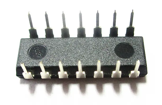
And there are some alternatives that can be choose. But it must to be remember: when selecting an equivalent, consider factors such as supply voltage, logic levels, speed.
How Many AND Gates are Contained in a 7408 NAND IC?
The 7408 IC contains four independent two-input AND gates. Each gate is designed to perform the logical AND operation, where the output is high only when both inputs are high. This quad AND gate configuration is one of the defining features of the 7408 IC, making it a versatile and widely used component in digital electronics.
Detailed Breakdown of the 7408 IC
The 7408 IC is structured as follows:
Gate 1:
Inputs: Pin 1 (Input A), Pin 2 (Input B)
Output: Pin 3
Gate 2:
Inputs: Pin 4 (Input A), Pin 5 (Input B)
Output: Pin 6
Gate 3:
Inputs: Pin 9 (Input A), Pin 10 (Input B)
Output: Pin 8
Gate 4:
Inputs: Pin 12 (Input A), Pin 13 (Input B)
Output: Pin 11
Applications of the 7408 IC's AND Gates
The 7408 IC, with its four independent two-input AND gates, is a versatile component used in various digital logic applications. The logical AND operation it performs is foundational in digital electronics, making the 7408 IC suitable for numerous practical uses. Below are some detailed applications of the 7408 IC's AND gates:
1. Digital Logic Circuits
In computing and digital systems, AND gates can be used to implement basic logical operations. For instance, in a combinational logic circuit, an AND gate might be used to ensure that an output is triggered only when all specified conditions are met. AND gates are crucial in the design of arithmetic circuits such as adders and multipliers as well. In a binary adder circuit, AND gates help manage carry operations, ensuring correct binary addition.
2. Control Systems
In an industrial setting, multiple sensors may monitor different parameters like temperature, pressure, and humidity. The outputs of these sensors can be fed into an AND gate to ensure that a machine only operates when all conditions are within acceptable ranges.
3. Digital Filters
AND gates can be used to implement digital filters that allow signals to pass through only when certain conditions are met. This can be useful in removing noise or unwanted signals from a digital stream.
4. Timing and Synchronization
In microprocessors and digital circuits, clock signals can be gated using AND gates to save power. The clock signal is allowed to pass only when the circuit needs to perform an operation. In addition, AND gates can combine multiple timing signals to create specific pulse shapes required for certain operations in digital electronics.
5. State Machines
State Transition Logic: Implement logic that dictates state transitions based on multiple inputs. This ensures that the system moves from one state to another only when all necessary conditions are satisfied.
Control Unit Design: In CPUs and other digital systems, control units use AND gates to manage the execution of instructions based on the current state and input signals.
6. Memory Address Decoding
AND gates are essential in memory address decoding applications, where they help in selecting specific memory locations based on address lines. For example, decode specific addresses in a memory array. When the correct combination of address lines is high, the corresponding memory location is selected for reading or writing data.
7. LED Displays and Indicators
AND gates can control LEDs that indicate the status of a system. For instance, an LED might light up only when multiple conditions are true, such as power being on and the system being operational. In multiplexed LED displays, AND gates can manage which segments of the display are lit based on the input conditions.
FAQs
Can IC 7408 be used for analog signals?
No, the IC 7408 is designed for digital signals only. Using it with analog signals may not yield accurate results.
How to check if the IC 7408 is working correctly?
You can use a multimeter to test the voltage at the output pins while providing known inputs. The output should follow the AND gate logic.
Is the 7408 IC compatible with CMOS logic levels?
No, the 7408 IC is a TTL device. Ensure that the input and output voltage levels are compatible with TTL logic.
What is the difference between the 7408 and 7432 ICs?
The 7408 IC contains AND gates, while the 7432 IC contains OR gates. They serve different logical functions.
Can the 7408 IC be used in low-power applications?
Yes, the 7408 IC consumes low power, making it suitable for various low-power digital applications.
Statement
All articles (images, texts, audio) on this site are uploaded and shared by users, or integrated from relevant internet sources, only for user's learning. If your rights are violated, please contact the administrator to delete! Link to this article: https://www.jinftry.com

