IC 7408 vs IC 7432: Definition, Truth Table and Pin Diagram
What is the Name of 7408 IC?
The 7408 IC is a well-known integrated circuit within the TTL (Transistor-Transistor Logic) logic family. It is specifically referred to as a Quad 2-input AND Gate IC. This designation highlights its core functionality and the specific configuration of its internal logic gates.

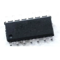
Integrated circuit 7408 contains four separate AND gates within a single 16-pin Dual In-Line Package (DIP). Each AND gate within the IC operates independently, so it can handle different logic operations simultaneously.
How Does IC 7408 Work?
The IC 7408 is a digital logic IC that implements the AND function. It has four independent AND gates, each with two inputs. When both inputs of an AND gate are high, the output is high. If either input is low, the output will also be low.
Each AND gate in the IC 7408 consists of bipolar junction transistors (BJTs) configured in a series arrangement. The essential principle behind the AND gate is that it only produces a high output (logic 1) when both of its inputs are high. Internally, the transistors within the gate act as switches. When both inputs are high, both transistors are fully turned on, allowing current to flow through the circuit and thus resulting in a high output. Conversely, if either input is low, at least one transistor will be off, blocking current flow and producing a low output.
The IC operates within the TTL (Transistor-Transistor Logic) voltage levels, typically powered by a 5V supply. Input voltages for logic high are generally between 2V and 5V, while logic low is between 0V and 0.8V. The output can drive standard TTL loads, ensuring it interfaces well with other logic devices.
In practical applications, it is essential to consider the power supply decoupling and heat dissipation for the IC 7408. Decoupling capacitors help filter out noise and stabilize the power supply, while proper heat management ensures the IC operates reliably without overheating. Accurate pin configuration and referring to the datasheet are crucial to avoid incorrect connections and ensure the IC functions as intended.
7408 IC Truth Table
Here's the truth table for the IC 7408, which outlines the behavior of the AND gates:
|
Input A |
Input B |
Output |
|
0 |
0 |
0 |
|
0 |
1 |
0 |
|
1 |
0 |
0 |
|
1 |
1 |
1 |
In this table, 0 represents a low voltage level, and 1 represents a high voltage level.
Integrated Circuit 7408 Symbol
The symbol for the IC 7408 is a rectangle with four AND gates represented inside it. Each gate is depicted with two inputs and one output. The pins are arranged to show the connections to each gate. The symbol is a standard representation for logic ICs, helping to visualize the internal structure and connections.

What is the PIN Configuration of IC 7408 AND Gate?
The pin configuration of the 7408 IC is arranged to accommodate the four AND gates and essential power supply connections. Here is a breakdown of its pinout:
Pin 1: Input A of Gate 1
Pin 2: Input B of Gate 1
Pin 3: Output of Gate 1
Pin 4: GND (Ground)
Pin 5: Input A of Gate 2
Pin 6: Input B of Gate 2
Pin 7: Output of Gate 2
Pin 8: VCC (Power Supply)
Pin 9: Input A of Gate 3
Pin 10: Input B of Gate 3
Pin 11: Output of Gate 3
Pin 12: GND (Ground)
Pin 13: Input A of Gate 4
Pin 14: Input B of Gate 4
Pin 15: Output of Gate 4
Pin 16: VCC (Power Supply)
Features of IC 7408 Chip
1. Low power consumption
2. TTL outputs
3. Recommended operating voltage is 5V
4. The maximum current allowed to draw through each gate output is 8mA
5. Operating voltage range of 4.75V to 5.25V
6. Maximum supply voltage of 7V
7. Typical fall time is 18ns
8. Typical rise time is 18ns
9. High noise immunity
10. Wide range of applications
What is the 7432 IC Name?
The 7432 IC is a Quad 2-input OR Gate integrated circuit. It also belongs to the 7400 series of digital logic ICs, which are widely used in electronic circuits for performing various logic functions. It contains four independent OR gates in a single package. The primary role of the 7432 is to perform the OR operation, which is fundamental in digital logic design.
7432 IC Pin Diagram
The 7432 IC is housed in a 14-pin Dual In-Line Package (DIP) with the following pin configuration:

Pin 1: Input A of Gate 1
Pin 2: Input B of Gate 1
Pin 3: Output of Gate 1
Pin 4: GND (Ground)
Pin 5: Input A of Gate 2
Pin 6: Input B of Gate 2
Pin 7: Output of Gate 2
Pin 8: VCC (Power Supply)
Pin 9: Input A of Gate 3
Pin 10: Input B of Gate 3
Pin 11: Output of Gate 3
Pin 12: GND (Ground)
Pin 13: Input A of Gate 4
Pin 14: Input B of Gate 4
Pin 15: Output of Gate 4
Pin 16: VCC (Power Supply)
IC 7432 Truth Table
The truth table for the IC 7432 OR gates is as follows:
|
Input A |
Input B |
Output |
|
0 |
0 |
0 |
|
0 |
1 |
1 |
|
1 |
0 |
1 |
|
1 |
1 |
1 |
How Do You Identify Pin Connections on an AND Gate IC Chip?
Identifying pin connections on an AND gate IC chip is crucial for ensuring proper functionality in electronic circuits. Here's a comprehensive guide on how to accurately determine and connect the pins of an AND gate IC:
1. Consult the datasheet
The most reliable method to identify pin connections is by consulting the IC’s data sheet. The data sheet provides detailed information about the IC, including pin configuration, electrical characteristics, and functional descriptions. For example, the data sheet for the IC 7408 will show the specific arrangement of pins for each AND gate within the package.
2. Refer to the pin diagram
ICs usually have a pin diagram on their packaging or in technical documentation. This diagram visually represents the pin arrangement and helps in quickly identifying each pin’s function. Generally, the diagram will show pin numbers around the IC’s outline, making it easier to locate specific pins.
3. Understand the pin configuration
For an AND gate IC like the 7408, the pin configuration is standardized within the 7400 series. For example, in the 7408, Pin 1 and Pin 2 are inputs for the first AND gate, and Pin 3 is the output.
4. Identify pin functions
These are where you connect the logic signals to be processed. For the 7408, they are generally positioned in pairs (e.g., Pins 1 and 2).
5. Use the IC markings
ICs are often marked with their part number and pin functions on the package itself. This information can provide a quick reference for pin identification.
6. Verify with a multimeter
If documentation is not available, a multimeter can be used to verify pin connections.
7. Refer to online resources
For additional confirmation, online resources and technical forums can provide practical insights and pin configurations for specific ICs. Websites like manufacturer’s support pages and electronics community forums often have detailed pin configuration information.
How to Connect IC 7408?
Connecting the IC 7408 involves several key steps to ensure proper operation and functionality in your circuit. Here’s a detailed guide:
1. Understand the Pin Configuration
The IC 7408 is packaged in a 16-pin Dual In-Line Package (DIP). To connect the IC properly, you first need to familiarize yourself with its pin configuration. The pins are arranged as follows: Pin 1 and Pin 2 are the inputs for the first AND gate, Pin 3 is the output for this gate, Pin 4 is the ground (GND), Pin 5 and Pin 6 are inputs for the second AND gate, Pin 7 is the output, and so on. Pins 8 and 16 are the VCC (power supply) pins, and Pins 4 and 12 are for ground.
2. Connect Power Supply and Ground
To power the IC, connect Pins 8 and 16 to the positive voltage supply, typically +5V. This provides the necessary power for the IC’s operation. Similarly, connect Pins 4 and 12 to the ground of your circuit. These ground connections provide a reference point for the logic levels and complete the circuit. Ensuring stable and correct power supply and ground connections is crucial for the IC’s proper functioning.
3. Connect the Inputs and Outputs
Each of the four AND gates in the IC has two input pins and one output pin. For the first AND gate, connect your input signals to Pin 1 (Input A) and Pin 2 (Input B). The output from this gate is available on Pin 3. Similarly, connect the inputs for the second gate to Pins 5 and 6, with the output on Pin 7. Repeat this for the remaining two gates. Ensure that the outputs are connected to the appropriate load or subsequent stage in your circuit to observe the results.
4. Use Decoupling Capacitors
To improve the stability of the IC and reduce noise, it’s advisable to use decoupling capacitors. Place a 0.1µF ceramic capacitor between the VCC (Pins 8 and 16) and GND (Pins 4 and 12) close to the IC. This capacitor helps filter out any power supply noise and stabilize the voltage, which is essential for reliable operation of the IC.
5. Ensure Proper Wiring
Before powering up the circuit, double-check all your connections. Verify that each pin is correctly connected according to its designated function. Ensuring that power and ground pins are properly connected and that inputs and outputs are correctly wired will help avoid any malfunction or damage to the IC. Secure all connections to prevent any loose or faulty wiring.
6. Test the Circuit
Once everything is connected, power up the circuit and test each AND gate. Apply different combinations of input signals and check the output. The output should be high only when both inputs are high for each gate. This test will confirm that the IC is working correctly and performing the AND logic operation as expected.
7. Troubleshooting
If the IC does not function as expected, start by checking the power supply voltage to ensure it is stable and within the specified range. Inspect all ground connections and verify they are secure. Check the input signals to ensure they are within the correct voltage levels. If the problem persists, confirm that the IC is correctly placed and that all pin connections are accurate.
Related Content
1. IC 7408 Equivalents: Datasheet and Pinout
2. IC 7408 Logic Gate Chip: Pin Diagram and Truth Table
3. IC 741 Op Amp: Pin Diagram, Working & Equivalents
Statement
All articles (images, texts, audio) on this site are uploaded and shared by users, or integrated from relevant internet sources, only for user's learning. If your rights are violated, please contact the administrator to delete! Link to this article: https://www.jinftry.com


