NMOS vs. PMOS: Symbol, Diagram, Working Principle, Structure, Truth Table

NMOS (N-channel Metal Oxide Semiconductor) and PMOS (P-channel Metal Oxide Semiconductor) are two basic field effect transistors (FETs) that are widely used in integrated circuit design. They differ in their role in the circuit, working principle, and application. This article will provide a detailed introduction to the characteristics, working principle, and application of NMOS and PMOS.
What is NMOS?
NMOS (N-channel Metal Oxide Semiconductor) is a field effect transistor (FET). It is one of the two basic MOSFET types, the other being PMOS (P-channel Metal Oxide Semiconductor).In an NMOS transistor, the channel through which current flows is created by applying a voltage to the gate terminal. This voltage creates an electric field that attracts electrons from the source terminal into the channel, and when enough voltage is applied between the two terminals, current flows from the drain to the source.
NMOS transistors are widely used in digital and analog circuits, for example in CMOS (Complementary Metal Oxide Semiconductor) technology, they are paired with PMOS transistors to create complementary logic gates and complex integrated circuits. Because they are fast, low power, and easy to integrate into semiconductor manufacturing processes, they are widely used in microprocessors, memory chips, and other digital logic circuits.
What is PMOS?
PMOS (P-channel metal oxide semiconductor) is a field effect transistor (FET) and one of the two basic MOSFET types, the other being NMOS (N-channel metal oxide semiconductor).In a PMOS transistor, the channel through which current flows is created by applying a voltage to the gate terminal. However, in a PMOS transistor, the channel carries positively charged "holes" instead of electrons. When a voltage is applied to the gate terminal, it creates an electric field that repels the holes out of the channel, and when enough voltage is applied between the two terminals, current flows from the source to the drain.
PMOS transistors are often used in complementary metal oxide semiconductor (CMOS) technology along with NMOS transistors. In CMOS circuits, PMOS transistors are used to implement logic functions that are complementary to NMOS transistors, allowing the construction of complex digital circuits with low power consumption and high noise immunity. PMOS transistors are used in a variety of applications, such as microprocessors, memory chips, and other integrated circuits.
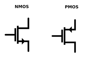
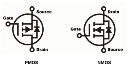
NMOS vs. PMOS: Symbols
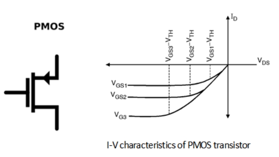
In both symbols, the arrows indicate the direction of current flow when the transistor is on. The arrows for NMOS and PMOS transistors are in opposite directions, reflecting the different types of charge carriers (electrons for NMOS and holes for PMOS) that make up the channel when the transistor is on.
NMOS vs. PMOS: How They Work?
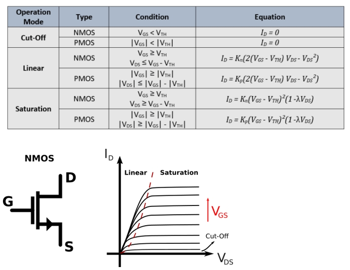
NMOS (N-channel Metal Oxide Semiconductor) and PMOS (P-channel Metal Oxide Semiconductor) transistors operate in a similar way, but they use different types of charge carriers and the direction of current flow.How NMOS Works?
- When a positive voltage (logic high) is applied to the gate terminal of an NMOS transistor relative to the source, it creates an electric field that attracts electrons toward the interface between the gate and the semiconductor substrate.
- This voltage creates an inversion layer or channel of n-type semiconductor material between the source and drain, allowing electrons to flow from the source to the drain when a voltage is applied between these terminals.
- When the gate voltage is high enough to create a channel, allowing current to flow between the source and drain, the transistor is in the "on" state. Conversely, when the gate voltage is low (logic low), the transistor is in the "off" state, and little current flows between the source and drain.
How PMOS Works?
- In contrast, when a negative voltage (logic low) is applied to the gate terminal of a PMOS transistor (relative to the source), it creates an electric field that repels holes from the interface between the gate and the semiconductor substrate.
- This voltage creates a depletion region or channel of p-type semiconductor material between the source and drain, and when a voltage is applied between these terminals, holes flow from the drain to the source.
- Similar to NMOS transistors, when the gate voltage is low enough to create a channel, the PMOS transistor is in the "on" state, allowing current to flow between the source and drain. Conversely, when the gate voltage is high (logic high), the transistor is in the "off" state, and little current flows between the source and drain.
In summary, NMOS transistors conduct current when a positive voltage is applied to the gate, while PMOS transistors conduct current when a negative voltage is applied to the gate. This fundamental difference in operation allows NMOS and PMOS transistors to complement each other in CMOS (Complementary Metal Oxide Semiconductor) technology, allowing the construction of a variety of digital logic circuits and integrated circuits.
NMOS vs. PMOS: Structure
The structures of NMOS (N-channel Metal Oxide Semiconductor) and PMOS (P-channel Metal Oxide Semiconductor) transistors are similar in many ways, but they differ in the type of semiconductor material used and the polarity of the majority charge carriers in the channel.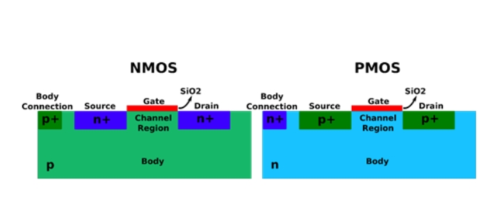
- Substrate: Both NMOS and PMOS transistors are typically fabricated on a silicon substrate.
- Gate: Both types of transistors have a gate terminal made of a conductive material such as polysilicon. The gate is insulated from the semiconductor substrate by a thin layer of insulating material (usually silicon dioxide), which is called the gate oxide.
- Source and Drain: These are the terminals through which current enters and exits the transistor channel. In an NMOS transistor, electrons flow from the source to the drain (hence the term "N-channel"), while in a PMOS transistor, holes flow from the drain to the source (hence the term "P-channel"). The source and drain regions are doped with impurities to create the desired conductivity type (n-type for NMOS and p-type for PMOS).
- Channel: The channel is the region between the source and drain that is controlled by the voltage applied to the gate. In an NMOS transistor, the channel consists of n-type semiconductor material, and electrons can flow when a voltage is applied to the gate. In a PMOS transistor, the channel consists of p-type semiconductor material, and holes can flow when a voltage is applied to the gate.
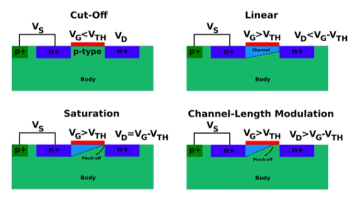
Overall, the key structural differences between NMOS and PMOS transistors are the polarity of the majority charge carriers in their channels, which determines the direction of current flow and the type of doping used in the source and drain regions.
NMOS and PMOS: Inverter, NAND Gate, NOR Gate Truth Table
1.Inverter
- The inverter is the most basic CMOS logic gate, consisting of an NMOS and a PMOS.
Truth Table:
Input (A)
Output (Y)
0
1
1
0
Working Principle:
When input A=0:
-
PMOS is turned on (because V_gs
- Output Y=1 (connected to VDD)
When input A=1:
- PMOS is turned off (because V_gs>V_th), NMOS is turned on (because V_gs>V_th).
- Output Y=0 (connected to GND)
2.NAND Gate:
- The NAND gate consists of two NMOS and two PMOS.
Truth table:
|
Input (A) |
Input (B) |
Output (Y) |
| 0 | 0 | 1 |
| 0 | 1 | 1 |
| 1 | 0 | 1 |
| 1 | 1 | 0 |
When input A=0 or B=0:
-
At least one PMOS is turned on (because V_gs
- Output Y=1 (connected to VDD).
When input A=1 or B=1:
- Both PMOS are turned off (because V_gs>V_th), and both NMOS are turned on (because V_gs>V_th).
- Output Y=0 (connected to GND).
3.NOR Gate
- NOR gates are also composed of two NMOS and two PMOS, but with different connection methods.
|
Input (A) |
Input (B) |
Output (Y) |
| 0 | 0 | 1 |
| 0 | 1 | 0 |
| 1 | 0 | 0 |
| 1 | 1 | 0 |
When input A=0 or B=0:
-
Both PMOS are turned on (because V_gs
- Output Y=1 (connected to VDD).
When input A=0 or B=1:
- At least one PMOS is turned off (because V_gs>V_th), and at least one NMOS is turned on (because V_gs>V_th).
- Output Y=0 (connected to GND).
NMOS vs. PMOS: Conduction Characteristics
The conduction characteristics of NMOS (N-channel Metal Oxide Semiconductor) and PMOS (P-channel Metal Oxide Semiconductor) transistors differ mainly in the type of charge carriers they use and the direction of current flow.NMOS and PMOS are widely used in CMOS logic gates, and through their complementary characteristics, various logic functions can be realized. Here is a summary:
- NMOS: Turns on when the gate voltage is greater than the threshold voltage, and the current flows from the drain to the source.
- PMOS: Turns on when the gate voltage is less than the threshold voltage, and the current flows from the source to the drain.
NMOS Conduction Characteristics
- Operation: Turns on when a positive voltage is applied to the gate terminal relative to the source terminal.
- Charge Carriers: Utilizes electrons as the majority charge carriers.
- Channel Creation: Applying a positive gate-source voltage attracts electrons to the interface between the gate and the semiconductor substrate, creating an inversion layer or channel of the n-type semiconductor material.
- Current Flow: When electrons pass through the channel under the influence of the electric field applied by the gate voltage, the current flows from the source to the drain.
PMOS Conduction Characteristics
- Operation: Turns on when a negative voltage is applied to the gate terminal relative to the source terminal.
- Charge Carriers: Utilizes holes as the majority charge carriers.
- Channel Creation: Application of a negative gate-source voltage repels holes from the interface between the gate and the semiconductor substrate, creating a depletion region or channel of the p-type semiconductor material.
- Current Flow: Current flows from the drain to the source as holes travel through the channel under the influence of the electric field applied by the gate voltage.
In summary, NMOS and PMOS transistors exhibit opposite conduction characteristics due to the polarity of the majority charge carriers in their channels and the direction of current flow in the on state.
NMOS vs. PMOS: MOS Switch Losses
For MOS switch losses, the key factor to consider is the resistance of the transistor when it is fully on. This resistance causes losses in the switch when conducting current. Here is a comparison of NMOS and PMOS transistors in this regard:NMOS
Since the mobility of electrons in semiconductor materials is generally higher than the mobility of holes, NMOS transistors tend to have a lower resistance in the conducting state.
Lower on-resistance results in lower conduction losses when the NMOS switch is fully on, thus improving efficiency.
PMOS
Due to the low electron mobility relative to hole mobility in semiconductor materials, PMOS transistors generally have higher resistance in the conducting state.
Higher on-resistance can cause higher conduction losses when the PMOS switch is fully on, which can result in slightly lower efficiency than NMOS switches.
In practical applications, the choice of NMOS and PMOS switches depends on various factors, such as the specific requirements of the circuit, including voltage level, current level, switching speed, and overall system efficiency. However, for high-frequency and high-efficiency applications, NMOS switches are usually preferred because of their lower on-resistance and conduction losses.
NMOS vs. PMOS: MOS Tube Drivers
In digital circuit design, MOS (metal oxide semiconductor) transistors, including NMOS (N-channel MOS) and PMOS (P-channel MOS), are often used as driver transistors to control the switching behavior of other MOS devices or provide driving force for signal lines. Here is a comparison of NMOS and PMOS transistors as MOS tube drivers:NMOS Drivers
When a logic high voltage is applied to the gate of an NMOS transistor, it turns the transistor off, allowing the signal line to be pulled to ground through a low resistance path, effectively driving the line to a low level.
NMOS drivers are suitable for driving signals or loads that require a reliable connection to ground.
In CMOS logic circuits, NMOS transistors are often used to switch and amplify signals on the low voltage side of the circuit.
PMOS Drivers
When a logic low voltage is applied to the gate of a PMOS transistor, it turns the transistor off, allowing the signal line to be pulled to the supply voltage (VDD) through a low resistance path, effectively driving the line to a high level.
PMOS drivers are suitable for driving signals or loads that require a strong connection to the supply voltage.
In CMOS logic circuits, PMOS transistors are often used to switch and amplify signals on the high side of the circuit.
In CMOS technology, NMOS and PMOS transistors are often used together to form a complementary pair, where one transistor handles the pull-up operation and the other handles the pull-down operation. This complementary configuration allows for efficient and low-power operation in CMOS logic circuits. The choice between NMOS and PMOS drivers depends on the specific requirements of the circuit, such as voltage levels, signal characteristics, and power consumption considerations.
NMOS vs. PMOS: Biasing
PMOS Biasing
In PMOS biasing, substrate biasing (also called reverse biasing) biases the substrate or body of the transistor relative to the supply voltage (Vdd for PMOS and Vss for NMOS) to reduce leakage current and improve overall device performance.
The body of a PMOS transistor is biased to a voltage above the power supply voltage (Vdd).
By biasing the substrate to a voltage above Vdd, the threshold voltage (Vth) of a PMOS transistor is effectively increased. This helps reduce leakage current because the transistor is less likely to turn on when it should be off.
The higher substrate bias voltage in PMOS helps enhance the performance of the transistor by minimizing leakage current and improving overall power efficiency.
NMOS Biasing
In contrast, in NMOS biasing, the substrate bias biases the body of the NMOS transistor to a voltage below ground (Vss).
By biasing the substrate to a voltage below Vss, the threshold voltage (Vth) of an NMOS transistor is effectively lowered. This reduces leakage current because the transistor is less likely to turn on when it should be off.
The lower substrate bias voltage in NMOS helps minimize leakage current and improves the efficiency of the transistor.
In summary, while both NMOS and PMOS biasing techniques aim to reduce leakage current by adjusting the substrate bias voltage, they achieve this goal in opposite ways due to their inherent differences in operation. PMOS biasing involves biasing the substrate to a voltage above Vdd, while NMOS biasing involves biasing the substrate to a voltage below Vss. These techniques help optimize transistor performance and minimize power consumption in integrated circuit designs.
Common MOS Transistor Models
N-channel MOS transistor
1.A2700 (surface mount)
Rated voltage: 30V
Current: 9A
On-resistance: 7.3mΩ
2.SI4336 (surface mount)
Rated voltage: 30V
Current: 22A
On-resistance: 4.2mΩ
3.SI4404 (surface mount)
Rated voltage: 30V
Current: 17A
On-resistance: 8mΩ
4.SI4410 (surface mount)
Rated voltage: 30V
Current: 10A
On-resistance: 14mΩ
5.IRF7831 (surface mount)
Rated voltage: 30V
Current: 16A
On-resistance: 0.004Ω
P-channel MOS transistor
1.A2716 (surface mount)
Rated voltage: 30V
Current: 7A
On-resistance: 11.3mΩ
2.SI4405 (Surface Mount)
Rated voltage: 30V
Current: 17A
On-resistance: 7.5mΩ
3.SI4425 (Surface Mount)
Rated voltage: 30V
Current: 9A
On-resistance: 19mΩ
4.IRF7424 (Surface Mount)
Rated voltage: 30V
Current: 8.8A
On-resistance: 22mΩ
5.BTS120 (Through Hole)
Rated voltage: 100V
Current: 19A
On-resistance: 100mΩ
Final words
In conclusion, the comparison between NMOS transistors and PMOS transistors reveals their complementary roles in electronic circuit design. NMOS transistors use electrons as the majority charge carriers, excel in pull-down operation, and are widely used in low-side switches. On the other hand, PMOS transistors utilize holes as the majority charge carriers and are suitable for pull-up operation and are applied in high-side switching. The combination of NMOS and PMOS transistors in CMOS technology has made it possible to develop complex digital systems with low power consumption and high performance. As technology continues to advance, the unique characteristics of NMOS and PMOS transistors will continue to play a key role in shaping the future of electronics.
Statement:
All articles (images, texts, audio) on this site are uploaded and shared by users, or integrated from relevant internet sources, only for user's learning. If your rights are violated, please contact the administrator to delete! Link to this article: https://www.jinftry.com
TNPW06031K80FEEA│ TNPW060328K4FEEA│ TNPW0603301RFEEA│ TNPW080516R2BETA│ TNPW0805210KBEEA│ TP3-470-R│ TRR03EZPF4021│ TS184F23IET│ TS3004ITD1033T│ TS924IN│ TSW-113-07-T-S│ TT500N18KOF│ TUW3J15RE│ TV06DT-15-19SC-LC│ TV07DZ-13-4SD-LC│ TV07DZ-17-35JB-LC│ TVP00DZ-23-35HA│ TVP00RK-25-187PC-P35│ TVP00RQW-25-8PD-LC│ TVPS00RF-25-7PD-LC│ TVS06RK-21-11HE-LC│ TVS06RS-19-35PC-LC│ TVS07RF-17-26JD-LC│ TX40AC90-1407│ TXD2SA-L-6V-4│ TXR40SJ00-1208BI│ U11J62CME22│ U23J37ZGE22│ UBW1H331MHD│ UEP1H3R3MDD1TD│ UMZ33KFHTL│ UPGH33-2838-6│ UPW2A331MHD1TN│ USUG1000-503J│ V18ZA05P│ V23050-A1012-A542│ V23061B1002A401│ V24B3V3H100BN3│ V24B8M200BN2│ V300B2C100A3│ V375B2H100AL│ V48A8T400B2│ V51031500000G│ V715A2510000G│ V72A28E400B2│ VA0301600000G│ VBO40-16NO6│ VE-2N3-MY│ VE-2TJ-EV│ VE-BNM-CY-B1│ VE-BW3-EW-S│ VE-J2H-IX│ VE-J30-CZ-B1│ VE-J5J-IY-F2│ VF3871500000G│ VFC375C5C100A│ VI-23F-MV-F4│ VI-23J-EW-B1│ VI-274-EW-F2│ VI-2T1-MY-S│ VI-2W2-CX-F4│ VI-B5B-CW-F1│ VI-B5B-MW-B1│ VI-BWD-CV-S│ VI-J0B-IZ-F4│ VI-J1R-CX-F3│ VI-J4K-CZ-F4│ VI-JNL-CY│ VI-JNL-MZ-F3│ VI-JV1-IY│ VJ0402D560JXXAJ│ VJ0603A6R8CXAAC│ VJ0603D3R6CLBAP│ VJ0805A330FXBPW1BC│ VJ0805D180FLAAJ│ VJ0805D330MXBAP│ VJ0805Y102MXACW1BC│ VJ1206A6R8CXEMC│ VJ1206Y222KXJCW1BC│ VSKE71-14P│ WP63GD│ WSL25125L000FEB│ X9401WV24-2-7_157│ XBHAWT-02-0000-0000T40F4│ XC6121A225ER-G│ XC6121E542ER-G│ XC6123C625MR-G│ XC6135C23D9R-G│ XC6210A482MR-G│ XC6222C281PR-G│ XC6501A161NR-G│ XC6501D23ANR-G│ XC6505A421ER-G│ XC6805B2E18R-G│ XC9257A32EER-G│ XPN9R614MC-L1XHQ│ XQ6VLX550T-L1RF1759I│ XTEAWT-00-0000-00000HGE2│ Y0006V0494QT9L│ Y000714K9250T9L│ Y0024157R330B0L│ Y07891K00000C0L│ Y112150R0000T0L│ Y1756800K000V0L│ YC158TJR-0724KL│ YC162-FR-071K58L│ YK4461903000G│ ZGP323LAS2804C│ ZTX558STOB│


