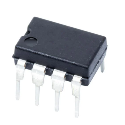
What is IC 741 Op Amp: Pin Diagram & Datasheet
IC 741 Operational Amplifier
The 741 IC op-amp is a widely used general-purpose operational amplifier that resembles a chip. The diagram of the 741 IC op-amp features 8 pins, with pins 2, 3, and 6 being the most critical. Pin 2 and Pin 3 are the inverting and non-inverting terminals, respectively, while Pin 6 represents the output voltage. The triangular symbol in the op-amp diagram signifies an operational amplifier integrated circuit, with the 741 op-amp being a well-known modern version.
Operational amplifiers, or op-amps, are essential in performing mathematical operations in various electronic circuits and are a common component of analog electronics. The 741 IC is constructed from multiple transistor stages, typically including a differential input stage, an intermediate gain stage, and a push-pull output stage. Differential op-amps usually consist of a matched pair of FETs (Field-Effect Transistors) or bipolar junction transistors.
IC 741 Pin Diagram
Understanding the pin configuration of the IC 741 is fundamental for designing circuits that utilize this operational amplifier. Each pin has a specific function, contributing to the overall performance of the IC. Here’s an in-depth look at each pin and its role:

Offset Null (Pin 1 and Pin 5)
These pins are used for offset voltage nulling. When there is a slight difference in voltage at the inputs even when they should be equal, the output will not be zero due to the inherent offset. Connecting a potentiometer between these two pins helps in adjusting and nullifying this offset, ensuring precise operation.
Inverting Input (−) (Pin 2)
The inverting input is one of the two differential inputs of the Op-Amp. When a signal is applied to this pin, it gets inverted at the output. This pin is crucial for configurations like inverting amplifiers, where the output is 180 degrees out of phase with the input signal.
Non-Inverting Input (+) (Pin 3)
This is the second differential input of the Op-Amp. Signals applied to this pin do not get inverted at the output. In non-inverting amplifier configurations, the output is in phase with the input signal. This pin is also used in many other applications where signal inversion is not desired.
VCC (+) (Pin 4)
This pin connects to the positive power supply. The voltage range typically goes up to +15V. It provides the necessary power for the Op-Amp to function. In dual power supply systems, this pin would connect to the positive voltage source.
Output (Pin 6)
The output pin delivers the amplified signal. It can source or sink current based on the input signal and the configuration of the Op-Amp. This pin is where the processed signal is available for further stages or for the final application, such as driving a speaker in audio applications.
VEE (−) (Pin 7)
This pin connects to the negative power supply or ground in single supply operations. The voltage range typically goes down to -15V. It completes the power supply circuit for the Op-Amp. In a dual power supply setup, this would connect to the negative voltage source.
No Connection (Pin 8)
Pin 8 is not internally connected to any part of the IC. It serves no functional purpose and can be left unconnected in the circuit design.
IC 741 Pin Configuration
l Pin 1 (Offset Null): Used for offset voltage adjustment.
l Pin 2 (Inverting Input): Receives the input signal for inversion.
l Pin 3 (Non-Inverting Input): Receives the input signal without inversion.
l Pin 4 (VCC +): Positive power supply input.
l Pin 5 (Offset Null): Used in conjunction with Pin 1 for offset voltage adjustment.
l Pin 6 (Output): Provides the output signal.
l Pin 7 (VEE -): Negative power supply input.
l Pin 8 (No Connection): Not connected internally, can be left floating.
Inverting Amplifier
The inverting amplifier configuration is a fundamental application of the IC 741 operational amplifier. In this setup, the input signal is applied to the inverting input (Pin 2) through a resistor (Rin). The non-inverting input (Pin 3) is connected to the ground. A feedback resistor (Rf) is connected between the output (Pin 6) and the inverting input (Pin 2). This configuration ensures that the output signal is an amplified version of the input signal, but inverted (180 degrees out of phase).
The voltage gain of the amplifier is given by the ratio -Rf/Rin, allowing for precise control over the amplification factor. This setup is widely used in applications requiring signal inversion and amplification, such as audio processing and signal conditioning.

Non-Inverting Amplifier
The non-inverting amplifier configuration with the IC 741 operational amplifier is designed to amplify the input signal without inverting it. The input signal is applied to the non-inverting input (Pin 3). The inverting input (Pin 2) is connected to a voltage divider network consisting of a feedback resistor (Rf) and a ground resistor (R1). The output (Pin 6) is fed back to the inverting input through Rf. This configuration ensures that the output signal is in phase with the input signal and provides an amplified version of it.
The voltage gain of the amplifier is given by 1+Rf/R1, offering flexibility in setting the desired gain. This setup is ideal for applications where maintaining the phase of the input signal is crucial, such as in sensor interfacing and buffer circuits.

Specifications of IC 741 Op-Amp
|
No. |
Specifications |
IC 741 Value |
|
1 |
Input offset voltage |
2mV |
|
2 |
Input bias current |
80nA |
|
3 |
Output impedance |
75Ω |
|
4 |
Slew rate |
0.5V/µs |
|
5 |
Input impedance |
2MΩ |
|
6 |
Gain bandwidth product |
1MHz |
|
7 |
Open-loop gain |
200,000 (106dB, typical) |
|
8 |
Output voltage swing |
±14V (with ±15V supply) |
|
9 |
Supply voltage range |
±3V to ±18V |
|
10 |
Operating temperature range |
0°C to 70°C |
|
11 |
Input voltage range |
-12V to +15V (with ±15V supply) |
|
12 |
Input noise voltage |
20nV/√Hz at 1kHz |
|
13 |
Total harmonic distortion |
0.015% at 1kHz |
|
14 |
Unity gain bandwidth |
1MHz |
|
15 |
Junction temperature |
150°C (maximum) |
Working Principle of IC 741 Op-Amp
The IC 741 operational amplifier functions by amplifying the voltage difference between its two input terminals, the inverting input (−) and the non-inverting input (+). The differential input stage of the IC 741 consists of a pair of transistors configured as a differential amplifier. This stage ensures that any common-mode signals (signals present on both inputs) are rejected, while the difference between the input signals is amplified. The high gain provided by the IC 741 allows it to respond effectively to even small differences in input voltage, making it highly sensitive and precise in its operation.
Following the differential input stage, the signal passes through one or more intermediate gain stages. These stages provide the necessary amplification, achieving an open-loop gain that is typically around 200,000 (106 dB). The high gain of the IC 741 ensures significant amplification of the input signal difference, although in practical applications, feedback mechanisms are used to control and stabilize the gain. The voltage follower stage, often included in the design, serves to buffer the high-gain stage, ensuring low output impedance and maintaining signal integrity.
The output stage of the IC 741 is designed to drive various loads effectively, typically using a complementary push-pull arrangement. This stage provides a wide output voltage swing, close to the supply rails, and ensures low output impedance, allowing for robust signal delivery. The operational amplifier operates with a dual power supply, usually ±15V, enabling it to handle both positive and negative swings of the output signal.
Internal Circuit Description of IC 741 Operational Amplifier
The internal structure of the IC 741 operational amplifier consists of several key components and circuits that work together to ensure high gain and stable amplification. Here’s a detailed look at the main parts:

l Input Stage with Transistors Q1 and Q2
The input stage of the IC 741 comprises transistors Q1 and Q2. Q1 is connected to the non-inverting input, and Q2 is connected to the inverting input. This differential pair helps to isolate the input signals and prevent feedback, ensuring that the amplifier responds accurately to the voltage difference between the inputs.
l Current Mirrors (Q8/Q9 and Q12/Q13)
Current mirrors, such as those formed by transistors Q8 and Q9, and Q12 and Q13, are used to regulate the current flow within the op-amp. These circuits ensure stable operation by maintaining consistent current levels, thereby minimizing the impact of input voltage fluctuations on the internal circuitry.
l Voltage Level Shifter (Q16)
The voltage level shifter, represented by transistor Q16, is responsible for reducing the voltage level from the amplifier circuit at the input section before passing it to the next stage. By doing so, it helps prevent signal distortion and maintains the integrity of the amplified signal throughout the stages of the op-amp.
l Class A Amplifier Stage (Q15, Q19, Q22) and Output Stage (Q14, Q17, Q20)
The class A amplifier stage, including transistors Q15, Q19, and Q22, along with the output stage consisting of Q14, Q17, and Q20, are crucial for amplifying the input signal and driving the output with sufficient power. The class A amplifier stage provides linear amplification, ensuring minimal distortion and high fidelity in the output signal. The complementary push-pull output stage enhances efficiency and provides a robust output capable of driving various loads.
l Offset Null Configuration (Q5, Q6, Q7)
The transistors Q5, Q6, and Q7 form part of the offset null configuration, allowing for offset null adjustment. This adjustment balances both the inverting and non-inverting inputs, minimizing any irregularities at the input phase of the differential circuit. Proper offset nulling is essential for precision applications, ensuring that the output remains accurate and free from unwanted offsets.
IC 741 Op-Amp Dimensions

IC 741 Op-Amp Applications
l Audio amplifiers - used in audio equipment for signal amplification.
l Signal conditioning - used in sensor interfacing to process and amplify signals.
l Active filters - implemented in low-pass, high-pass, band-pass, and band-stop filters for signal processing.
l Voltage followers (Buffers) - employed to provide impedance matching and prevent signal loading.
l Summing amplifiers - used in applications where multiple signals need to be combined into one output.
l Differential amplifiers - ideal for applications requiring the amplification of the difference between two signals.
l Integrators and differentiators - used in analog computers and signal processing for performing mathematical operations.
l Oscillators - used to generate sine, square, and triangular waveforms in signal generators.
l Comparator circuits - used in zero-crossing detectors, level shifters, and other threshold detection applications.
l Voltage regulators - used in power supplies to maintain a constant output voltage.
l PWM controllers - employed in motor control and power regulation applications.
IC 741 Datasheet
The datasheet includes parameters like input offset voltage, bias current, and slew rate, crucial for designing precise circuits, download IC 741 datasheet here: LM741CN.
Frequently Asked Questions (FAQs)
What is the main use of IC 741?
IC 741 is primarily used in analog signal processing applications.
Can IC 741 be used in high-frequency applications?
No, it is best suited for low-frequency applications due to its limited bandwidth.
What are the power requirements for IC 741?
It typically requires a dual power supply of ±15V.
How does an inverting amplifier work with IC 741?
An inverting amplifier inverts and amplifies the input signal based on the feedback resistor ratio.
What are the common applications of IC 741 Op-Amp?
IC 741 is used in audio amplifiers, signal conditioning, mathematical operations, oscillators, and filters.
Read more
1. IC 741 Op Amp: Pin Diagram, Working & Equivalents
2. Op Amp IC 741 Basics, Characteristics, Pins & Applications
3. IC 7408 Equivalents: Datasheet and Pinout
4. What is Diode - Definition, Diode Symbol, Functions
5. A Fully Introduction to Capacitor Symbols
Statement
All articles (images, texts, audio) on this site are uploaded and shared by users, or integrated from relevant internet sources, only for user's learning. If your rights are violated, please contact the administrator to delete! Link to this article: https://www.jinftry.com


