Lattice Semiconductor Corporation LFSCM3GA15EP1-6FN256I

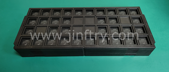
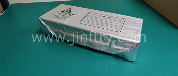
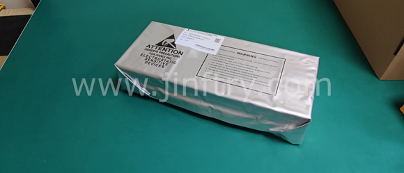
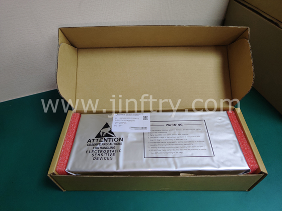
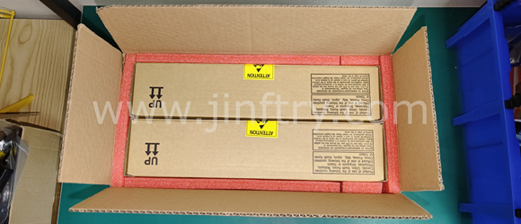
The picture is for reference only, please refer to the product specification
- LFSCM3GA15EP1-6FN256I
- Lattice Semiconductor Corporation
- IC FPGA 139 I/O 256FBGA
- Embedded - FPGAs (Field Programmable Gate Array)
- LFSCM3GA15EP1-6FN256I Datasheet
- 256-BGA
- Tray
-
 Lead free / RoHS Compliant
 - 1702
- Spot Inventory / Athorized Dstributor / Factory Excess Stock
- 1 year quality assurance 》
- Click to get rates
Delivery Services:

Payment Methods:

| Part Number LFSCM3GA15EP1-6FN256I |
| Category Embedded - FPGAs (Field Programmable Gate Array) |
| Manufacturer Lattice Semiconductor Corporation |
| Description IC FPGA 139 I/O 256FBGA |
| Package Tray |
| Series SCM |
| Voltage - Supply 0.95V ~ 1.26V |
| Operating Temperature -40°C ~ 105°C (TJ) |
| Mounting Type Surface Mount |
| Package / Case 256-BGA |
| Supplier Device Package 256-FPBGA (17x17) |
| Number of I/O 139 |
| Number of Gates - |
| Number of LABs/CLBs 3750 |
| Number of Logic Elements/Cells 15000 |
| Total RAM Bits 1054720 |
| Package_case 256-BGA |
LFSCM3GA15EP1-6FN256I Guarantees


• Prompt Responsiveness
• Guaranteed Quality
• Global Access
• Competitive Market Price
• One-Stop support services of supply chain
Jinftry, Your most trustworthy component supplier, welcome to send us the inquiry, thank you!
Do you have any questions about LFSCM3GA15EP1-6FN256I ?
Feel free to contact us:
+86-755-82518276
+8615019224070, annies65, +8615118125813
568248857, 827259012, 316249462
+8615019224070, +8615118118839, +8615118125813
( Email first will be appreciative )
LFSCM3GA15EP1-6FN256I Related Products