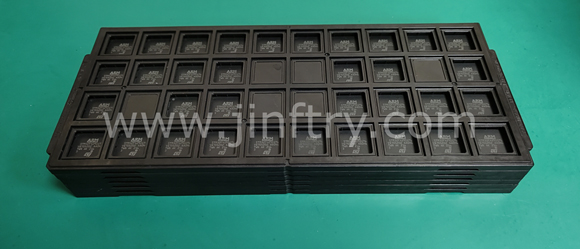
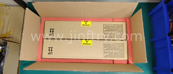
OR3T807PS240-DB Product Introduction:
Lattice Semiconductor Corporation Part Number OR3T807PS240-DB(Embedded - FPGAs (Field Programmable Gate Array)), developed and manufactured by Lattice Semiconductor Corporation, distributed globally by Jinftry. We distribute various electronic components from world-renowned brands and provide one-stop services, making us a trusted global electronic component distributor.
OR3T807PS240-DB is one of the part numbers distributed by Jinftry, and you can learn about its specifications/configurations, package/case, Datasheet, and other information here. Electronic components are affected by supply and demand, and prices fluctuate frequently. If you have a demand, please do not hesitate to send us an RFQ or email us immediately sales@jinftry.com Please inquire about the real-time unit price, Data Code, Lead time, payment terms, and any other information you would like to know. We will do our best to provide you with a quotation and reply as soon as possible.
Introducing the Lattice Semiconductor Corporation OR3T807PS240-DB, a cutting-edge programmable logic device designed to revolutionize the world of digital electronics. With its advanced features and versatile applications, this product is set to redefine the way we approach complex digital designs.
The OR3T807PS240-DB boasts an impressive array of features that make it a standout in the market. With a high-density architecture and 240 macrocells, this device offers unparalleled flexibility and scalability. Its low power consumption and high-speed performance make it ideal for a wide range of applications, from consumer electronics to industrial automation.
This programmable logic device is equipped with advanced security features, ensuring the protection of sensitive data and intellectual property. Its robust design and reliability make it suitable for mission-critical applications, where failure is not an option.
The OR3T807PS240-DB is compatible with industry-standard design tools, making it easy to integrate into existing workflows. Its user-friendly interface and intuitive programming options make it accessible to both seasoned professionals and newcomers to the field.
With its wide range of applications, the OR3T807PS240-DB is a versatile solution for various industries. From telecommunications and automotive to aerospace and defense, this device can handle the most demanding tasks with ease.
In conclusion, the Lattice Semiconductor Corporation OR3T807PS240-DB is a game-changer in the world of programmable logic devices. Its advanced features, versatile applications, and robust design make it a must-have for anyone looking to push the boundaries of digital electronics.
Field-Programmable Gate Array (FPGA) is an integrated circuit whose core is an array of programmable logic units, which can be connected through a network of programmable interconnects to form complex digital circuits. Each logical unit contains lookup tables (LUTs), triggers, and other basic logical elements that can be configured to perform various logical operations. This structure allows the FPGA to be programmed by the user after the factory to implement specific logic functions, and can be reprogrammed multiple times to suit different application needs.
Application
FPGA (Field-Programmable Gate Array) The primary role of FPGas is to provide powerful parallel processing capabilities and a high degree of flexibility. The application field of FPGA is extremely wide, covering almost all electronic systems requiring high performance and high flexibility. In the field of communication, FPGA is used to achieve high-speed data processing, protocol conversion, data compression and other functions to improve the performance and stability of communication systems. In terms of digital signal processing, the parallel processing capability of FPGA makes it an ideal choice for audio processing, video codec, image processing and other fields. In addition, FPgas are also widely used in industrial automation, automotive electronics, aerospace, medical equipment and other fields to achieve complex control and data processing tasks.
D882 Transistor Pinout, Equivalent, Uses and Datasheet
What is a D882 Transistor? The D882 is a popular NPN bipolar junction transistor (BJT) from the "D" series. It's designed for general-purpose amplification and switching in electronic circuits.
L7805CV Transistor: Pinout, Datasheet and Applications
What is the L7805CV Transistor? The ST model L7805CV is a voltage regulator in a three-end regulator TO-220 package that can be used in a wide range of applications. It ensures a steady 5V output from a higher input voltage. If sufficient heat dissipation is provided, the L1981301772 can provide an output current of more than 1A. Although these devices are primarily designed as fixed voltage regulators, they can be used with external components to obtain adjustable voltages and currents.
What is IC 741 Op Amp: Pin Diagram & Datasheet
The 741 IC op-amp is a widely used general-purpose operational amplifier that resembles a chip. The diagram of the 741 IC op-amp features 8 pins, with pins 2, 3, and 6 being the most critical. Pin 2 and Pin 3 are the inverting and non-inverting terminals, respectively, while Pin 6 represents the output voltage. The triangular symbol in the op-amp diagram signifies an operational amplifier integrated circuit, with the 741 op-amp being a well-known modern version.
IC 741 Op Amp: Pin Diagram, Working & Equivalents
What is LM741 Op-amp IC? The IC 741 chip is a classic operational amplifier integrated circuit (OP-AMP) chip, which has a wide range of applications. It was introduced by Texas Instruments in 1968 and is still widely used today.

 Lead free / RoHS Compliant