XC3SD3400A-5FGG676C Product Introduction:
Xilinx Inc. Part Number XC3SD3400A-5FGG676C(Embedded - FPGAs (Field Programmable Gate Array)), developed and manufactured by Xilinx Inc., distributed globally by Jinftry. We distribute various electronic components from world-renowned brands and provide one-stop services, making us a trusted global electronic component distributor.
XC3SD3400A-5FGG676C is one of the part numbers distributed by Jinftry, and you can learn about its specifications/configurations, package/case, Datasheet, and other information here. Electronic components are affected by supply and demand, and prices fluctuate frequently. If you have a demand, please do not hesitate to send us an RFQ or email us immediately sales@jinftry.com Please inquire about the real-time unit price, Data Code, Lead time, payment terms, and any other information you would like to know. We will do our best to provide you with a quotation and reply as soon as possible.
Introducing the Xilinx Inc. XC3SD3400A-5FGG676C, a cutting-edge programmable logic device that revolutionizes the world of digital design. This advanced FPGA (Field-Programmable Gate Array) offers unparalleled performance and versatility, making it the ideal solution for a wide range of applications.
The XC3SD3400A-5FGG676C boasts an impressive array of features that set it apart from the competition. With a generous capacity of 3,400 slices and 5,000 logic cells, this FPGA provides ample resources for complex designs. Its high-speed interfaces, including 10/100/1000 Ethernet and PCI Express, enable seamless connectivity and data transfer. Additionally, the device supports a wide range of I/O standards, ensuring compatibility with various peripherals.
This FPGA is designed to excel in diverse application fields. In the telecommunications industry, it can be used for high-speed data processing, network acceleration, and protocol conversion. In the automotive sector, it enables advanced driver assistance systems, infotainment, and vehicle networking. In the industrial automation domain, it facilitates real-time control, machine vision, and robotics. Furthermore, the XC3SD3400A-5FGG676C is well-suited for aerospace and defense applications, such as radar systems, avionics, and secure communications.
With its exceptional performance, extensive feature set, and broad application range, the Xilinx Inc. XC3SD3400A-5FGG676C is the ultimate choice for engineers and designers seeking a powerful and flexible FPGA solution. Stay ahead of the curve and unlock limitless possibilities with this state-of-the-art programmable logic device.
Field-Programmable Gate Array (FPGA) is an integrated circuit whose core is an array of programmable logic units, which can be connected through a network of programmable interconnects to form complex digital circuits. Each logical unit contains lookup tables (LUTs), triggers, and other basic logical elements that can be configured to perform various logical operations. This structure allows the FPGA to be programmed by the user after the factory to implement specific logic functions, and can be reprogrammed multiple times to suit different application needs.
Application
FPGA (Field-Programmable Gate Array) The primary role of FPGas is to provide powerful parallel processing capabilities and a high degree of flexibility. The application field of FPGA is extremely wide, covering almost all electronic systems requiring high performance and high flexibility. In the field of communication, FPGA is used to achieve high-speed data processing, protocol conversion, data compression and other functions to improve the performance and stability of communication systems. In terms of digital signal processing, the parallel processing capability of FPGA makes it an ideal choice for audio processing, video codec, image processing and other fields. In addition, FPgas are also widely used in industrial automation, automotive electronics, aerospace, medical equipment and other fields to achieve complex control and data processing tasks.
AXP2101 Introduction, Data Analysis and Datasheet PDF
AXP2101 is a high-performance, low-power power management chip (PMIC) widely used in various portable electronic devices. The chip is designed and manufactured by Beijing Jingfeng Mingyuan Semiconductor Co., Ltd., and its main function is to provide efficient power management solutions for the system. AXP2101 integrates multiple power management functions, including battery charge management, voltage regulation, power path management and multiple protection functions.
IC 7490 Decade Counter: Pin Diagram, Working & Features
What Does IC 7490 Represent? The IC 7490 is a decade counter, meaning it counts in decimal (base-10) from 0 to 9. This counting capability is achieved through a series of flip-flops, which divide the input frequency by 10. The IC 7490 is designed for use in digital circuits where a count of 10 is needed.
What is IC 741 Op Amp: Pin Diagram & Datasheet
The 741 IC op-amp is a widely used general-purpose operational amplifier that resembles a chip. The diagram of the 741 IC op-amp features 8 pins, with pins 2, 3, and 6 being the most critical. Pin 2 and Pin 3 are the inverting and non-inverting terminals, respectively, while Pin 6 represents the output voltage. The triangular symbol in the op-amp diagram signifies an operational amplifier integrated circuit, with the 741 op-amp being a well-known modern version.
7404 IC: Comprehensive Guide on Datasheet, Pin Diagram, Applications
What is the 7404 IC? The 7404 IC, commonly known as SN7404 hex inverter, it is a hex inverter integrated circuit commonly used in digital electronics. As a member of the 7400 series of integrated circuits, it plays a critical role in various logic gate designs. The 7404 IC is a hex inverter, meaning it contains six individual inverter gates. In digital logic, an inverter, or NOT gate, is a fundamental building block that outputs the opposite logic level to its input.

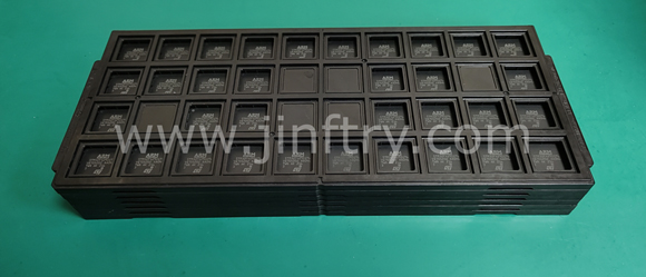
 Lead free / RoHS Compliant